- Hearing Aid
- Amplified Ear
- A Low Cost Hearing Aid
- Studio Series Stereo Headphone Amplifier
- Stereo Headphone Amplifier Circuit Schematic
- Pure Class-A Headphone Amplifier Schematic
- Portable Headphone Amplifier Circuit
- A Hiqh Quality Headphone Amplifier Schematic
- Ultra-High Fidelity High Power Amplifier Reference Design
- Speach Amplifier
- DC-Coupled Audio Amplifier
- A Low Power Wireless Audio Power Amplifier
- 8 Watt Audio Power Amplifier Schematic
- 7 Watt Audio Power Amplifier Circuit Schematic
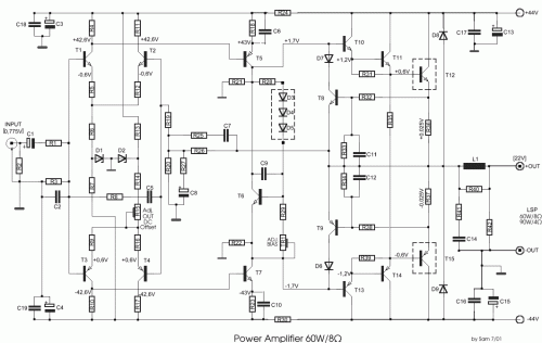
- 60 Watt Audio Power Amplifier Circuit Diagram
Power amplifier 60W/8Ω
Description
This circuit was designed and manufactured the '80's. From then it works without problem. It does not present any particular constructional problem, beyond known: the attention in the provided force of power supply - choice suitable heatsink and good matching of drivers transistor. Diodes D3 5 should be placed above in heatsink of the power transistors, so that they have thermic coupling with the output transistors. With the trimmer R15, we regulate the continuous voltage, in the exit of amplifier [that works few time and is stabilised thermic ]. With the trimmer TR1, we regulate the bias current of amplifier in the 50 until 100 mΑ. The bias current we can him measure if we measure the fall of voltage in utmost resistances R36 and R37, for the voltage that are given in the circuit the current are roughly 75 mΑ. The voltage that are reported in the drawing are original, but they can they have a tolerance of order ± 10%.
Circuit diagram
Parts list
- R1=1.8Kohm
- R2=220Kohm
- R3=27Kohm
- R4-10-11-17=3.3Kohm
- R5-9-12-16=100ohm
- R6=18Kohm
- R7-13=3.9Kohm
- R14=10Kohm
- R15=22Kohm Trimmer
- R18-23=330ohm
- R19-21-22=15Kohm
- R20=12Kohm
- R24-30=82ohm
- R25=8.2Kohm
- R26=27Kohm
- R27=820ohm
- R28=3.3Kohm
- R29=100ohm
- R31-39=180ohm
- R32-38=6.8Kohm
- R33-34=1.2Kohm
- R35=82ohm /1W
- R36-37=0.33ohm / 5W
- R40-41=10ohm / 2W
- R42=180ohm/5W
- TR1=4.7Kohm Trimmer
- D1-2=24V/1W Zener
- D3....9=1N4002
- T1-2=BC550C
- T3-4=BC560C
- T5-13=BD530
- T6-8=BC414C
- Τ9=BC416C
- T7-10=BD529
- T11=BD591
- T14=BD592
- T12=2N5630
- T15=2N6030
- C1=4.7uF/25V
- C2=470pF
- C3-4=100uF/63V
- C5=68pF
- C6-10=330pF
- C7=22pF
- C8=220uF/16V
- C9=100nF 100V
- C11-12=10pF
- C13-15=47uF/63V
- C16-17=100nF/100V
- C18-19=100nF/100V
